Showing posts with label MICROWIND. Show all posts

9.6.10

MICROWIND + DSCH COMPLETE WITH EXAMPLES ( Full Version with 6 metal layers)

microwind
Design FlowMICROWIND supports entire front-end to back-end design flow.
For front-end designing, we have DSCH (digital schematic editor) which posses in-built pattern based simulator for digital circuits. User can also build analog circuits and convert them into SPICE files and use 3rd party simulators like WinSpice or pSPICE.
DSCH can convert the digital circuits into Verilog file which can be further synthesized for FPGA/CPLD devices of any vendor. The same Verilog file can be compiled for layout conversion in MICROWIND.
The back-end design of circuits is supported by MICROWIND. User can design digital circuits and compile here using Verilog file. MICROWIND automatically generates a error free CMOS layout. Although this place-route is not optimized enough as we do not indulge in complex place & route algorithms.
User can also create CMOS layout of their own using compile one line Verilog syntax or custom build the layouts by manual drawing.
The CMOS layouts can be verified using inbuilt mix-signal simulator and analyzed further for DRC, crosstalks, delays, 2D cross section, 3D veiw, etc.
MICROWIND is truly integrated EDA software encompassing IC designs from concept to completion, enabling chip designers to design beyond their imagination. MICROWIND integrates traditionally separated front-end and back-end chip design into an integrated flow, accelerating the design cycle and reduced design complexities.
It tightly integrates mixed-signal implementation with digital implementation, circuit simulation, transistor-level extraction and verification – providing an innovative education initiative to help individuals to develop the skills needed for design positions in virtually every domain of IC industry.

MICROWIND  +  DSCH  COMPLETE  WITH

EXAMPLES   ( CLICK  TO  DOWNLOAD)

 or

CLICK HERE TO DOWNLOAD – MICROWIND V3.1 only


MICROWIND LAYOUT TIPS

Tips on the finger Tips:
In this post we will be looking at various design optimization tips.
The courtesy to most of these tips are SSN sir. Thank you sir.

1.  While drawing the layouts, its best practice to have a single Vdd/Vss rail running.
How do we do this?
Draw a simple metal rail. Give Vdd/Vss to it and tap it wherever you need.
So far we haven't come across this. But in the future layouts, we will be making use of this.

2.  Avoid digging unnecessary wells.
Yeah its pretty simple for us to draw as many n well as possible. But implementing this at industry level is not possible. In industry they go for laying all p devices in a single n well. You may notice that we have used the same practice in design of Transmission Gate.

3.  Avoid using poly for routing.
Though we have made use of poly for routing in design of TG, its not a good practice. Its better to use metal for this purpose. Use of metal will reduce resistance.

4.  More tips will follow based upon inputs from experts.

MICROWIND Tutorial Part 7 : Design and Layout of D Flip Flop


The D flip flop shown above is very much different from what we have learnt so far. We have designed it using Nand nor or some other basic gates. But this is completely different.

You can also see that the circuit is like cascading of two similar blocks. Block one includes M1, M2 and the first 2 inverters. The rest of the circuit is the repetition of the first part.
 
Now, why all this unnecessary fuss? Just to make our life simple. If we draw the first part, then we just need to do our Ctrl+C and Ctrl+V to get the second part. As simple as that.

Back to business: As you can see in the schematic, the circuit involves only two basic elements. An nMOS and an inverter. Basically you need to draw only these two and half of your headache is over. (No kidding, I swear J )

step 1:
The first step is of course opening the Microwind.


Step 2:
From the palette click on the Moss generator and click Generate device. Check the lambda box (bottom right). Make the Width MOS equal to 4. Now click on Generate device. Click bindass at any place on the screen. We get an nMOS.


Step 3:
You can see that the clock which we are using is of two types. One is clk and the next is its complement. That is clk_bar. For that we need an extra inverter. (Other than the four visible). I won’t be showing you how to draw and inverter. You can refer to the previous tutorial to get the idea regarding that. We will be directly inserting it. (Cool eh?).

Go to file>Insert Layout. Browse to the previously drawn inverter and here you are.

You should be able to see the screen somewhat like this:


Insert another inverter. This is Inv 1. You can refer the schematic. This inverter is connected to the output of the nMOS M1.
We need to name them as we draw. This will make lesser confusions.


Step 4:
Half the work is over. The only thing that we need to do is placing them properly. Copying and pasting them on the right area in the right manner. You owe me a treat for this simplicity.
We will be drawing everything in a single well. This will reduce the delay and make it a best choice for the counters and register designs.
We need to take a little care now. Remember that we need to maintain a minimum of 4 lambda distance between adjacent metal rails.
So, be little careful while placing. Keep doing DRC at each step to make sure that you haven’t ended up doing it wrong.

The layouts placing:
  1. Place the Inverter for inverting the clock at extreme left. (It’s not visible in the schematic, but we need to draw it for inverting the clock and getting clk_bar.
  2. Now, everything else will be according to the schematic. Place a pass transistor, i.e. an nMOS (M1) at a distance of 4λ from the inverter.
  3. To the right of this MOS, we have another inverter named Inv 1. Place it at a distance of 4λ from it. Please make sure that all nMOS and pMOS are at the same level.
  4. The output of this Inv 1 inverter is connected to the input of Inv 2 inverter. So we need to place Inv 2 to the right of Inv 1 at a distance of 4λ. (If you are getting confused scroll up and see the schematic)
  5. The output of Inv2 is connected as input to pass transistor M2. So, place a pass transistor nMOS M2 to the right of Inv 2.
 
At this point the layout should look somewhat like this.


The intermediate file can be found here:


Step 5:

As you can make out, we have just done with placing. We need to connect the devices now. Also note that, we have not drawn the second half. Once we are done with the connection, we will duplicate first half. (Both first and the second stages are identical).

Follow this convention:

The vertical routing should be done with metal 2.
The horizontal routing to be done with metal 1.
Note that you should use Metal 1 to Metal 2 contact to connect to metal 1 and metal 2. (It can be found in the palette)
Care should be taken while connecting a polysilicon layer to metal 2 layers. A polysilicon layer cannot be connected to metal 2 layers directly. First, it has to be connected to metal 1. And then it has to be connected to metal 2.
With the above things in our mind, we will proceed with the connections.
 
After the connections, the layout will look somewhat like this.


You can even download this intermediate file and analyze it.


Step 6:
It’s time to go for stage 2. Copy the layout, just before first inverter and place it to the right of the existing layout.
This creates the second stage.
Again do the necessary connections and your layout is ready.


The final layout will look similar to this.


You can find the same over here:
The output waveforms looks like this:


You can cascade this layout in the manner you want and create various registers and counters.

Have  a  great   time

MICROWIND Tutorial Part 6 : Design and VLSI layout of Schmitt Trigger circuit.

Schmitt Trigger. (Never omit the "c" and "t" from the name of this circuit).
Yes, very soon we are back with a hot tutorial on Schmitt trigger. As usual, we will be providing the layout and simulation waveforms. Some of them are really sleeping off by the time we are done with the explanation, so we are cutting short the explanation and just giving pictorial hints so that you can draw on your own. Reffer back to the previous tutorial incase you need some basic guidance.

In electronics, a Schmitt trigger is a comparator circuit that incorporates positive feedback.
When the input is higher than a certain chosen threshold, the output is high; when the input is below another (lower) chosen threshold, the output is low; when the input is between the two, the output retains its value. The trigger is so named because the output retains its value until the input changes sufficiently to trigger a change. This dual threshold action is called hysteresis, and implies that the Schmitt trigger has some memory. In fact, the Schmitt trigger is a bistable multivibrator.

Schmitt trigger devices are typically used in open loop configurations for noise immunity and closed loop positive feedback configurations to implement multivibrators.(Courtesy: Wikipedia)
You can read the entire article over here.

Here is the schematic. Please go through the schematic properly. The naming conventions used in the schematic(for naming the MOS devices) are retained in the layout for readability.


The desing is very simple. Using the MOS generator place few n and p device and provide proper routing.
Here is the explainatory layout of Schmitt Trigger Circuit:


The output waveforms (voltage vs time) can be observed as follows:


But we are less interested in this. We want to see the hysteresis curve. To viewe the hysteresis curve follow the instructions:
1. Click on Voltage vs Voltage at the bottom of the simulation screen. (Marked with red circle in the next figure)
2. Tick the Hysteresis right at the right corner of the screen. (Again it is highlighted in the next figure)
3. Click on Reset followed by More.
You are done with Schmitt Trigger and you should be able to see the hysteresis curve as follows.


Final Schmitt Trigger Layout:


Have a great time

MICROWIND Tutorial Part 5 : Three (3) Input NAND gate

The schematic and stick diagram of 3 input nand gate looks something like this:


Please post a comment if you want to know the working of the three input nand gate. I will be more than happy to explain.

Step by step layout for 3 input nand gate.

1.     1.   Draw a single pMOS from MOS generator (available in palette)


2.     2.  Select on units in lambda (underlined in the following figure) Keep the    length as 2λ and width as 4λ.
3.    
3.  3.  Copy and place them side by side or just create two more pMOS

4.   4.  Place them beside each other at a distance of 4λ.(refer figure). Note that we need to draw them in parallel, as shown in the schematic.


5.       Now we need nMOS in series. You can of course use MOS generator and extend and draw the polysilicon sticks as shown below


6.     5. By this time we have 3 pmos and 3 nmos generated. Join the corresponding gates. Give Vcc and Vdd and the input signals.

7.       The final diagram should look like one below.


8.       
WWe are done again.


9.   The waveforms observed are:


    Have a great time.

MICROWIND Tutorial Part 4: Design, Layout and Application of CMOS Buffer

You can get a detailed idea of buffer here


Here is a logic diagram of buffer. As you can see, it is basically two inverters connected in series. This but obiviously results in no change in the output. (Complement of Complemented signal is the original signal). Then why use it?
 
Not all the time in a circuit we connect Vdd(Poser supply) to each and every node. This is because they dont need it. (because of the design). So, after a certain length of devices, the logic levels starts degrading. The high level starts reducing from that of Vdd value. Such a degradation causes noisy output and many error. Therefore the signal needs boosting. This boosting is provided by the buffer. 
In few circuits, it can be used to hold the value of a signal for certain duration.
It is used and a separation element between two different circuitry to eliminate cross talk or unwanted noise.
Enough of applications? If you need more, comment to this article. I will be glad to post few more.
I will not be going in much detail regarding the layout of the buffer. You can reffer to part 2 (design of the inverter) to get a detailed design viewe of the inverter.
 
I will be just posting the steps and the final layout.
 
Step1: (Not open the favourite Microwind window..blah blah blah)
Make a copy of the inverter circuit which you have drawn. Open the copy Microwind>File>Open. Browse to the layout and open it.
You have got one inverter. We need the next one.
 
 
Step 2:
Shortcut 1: Import an inverter. Go to File>Insert Layout browse to the inverter and import it.
Shortcut 2: In the top menu, click on Copy element. Drag the mouse holding the left button over the layout till its completely selected. Release left mouse button. You should be able to see a dotted layout exactly same as the one you have just copied. Place it away. If you happen to commit a mistake, Ctrl+U will undo it. :). The recommended spacing between them is 7lambda. You may do DRC once to find the exact spacing.
 
 
Step3:
Routing:
Ahem. Forgot to write almost final step :). Yes, we are almost done (again).
Here we will be using Vdd and Vss for both the inverters. This is as good as supplying 2 power supplies. For example, we have a single UPS for the whole computer. This is like supplying separate UPS for monitor and CPU.
We are not that rich, or are we?:).
So, what we do is draw single rail at the top of the layout, and give a single Vdd to it. Later, we can tap Vdd from it. We do the same for Vss.
Now, we need to connect the output of the first inverter to the input of the second. This can be done in two ways. Using polysilicon (because the distance is less, if the distance is more, it introduces unnecessary patasitics) or using metal.
 
I have used metal. Connect the layers. Do the dew( I mean DRC). Thats it. The layout should look something like this:


Press the simulation button. You should get the waveforms as shown in the fugure. If you dont, check the contacts and debug it. All the best.


Have a cup of coffe and be ready for the next session.
See you soon.
Keep watching this space for more.
Have a nice day.

Microwind Tutorial Part3: Design of Transmission Gate (Import layout, save time)

We are back this time with a tutorial on layout of transmission gate (TG).
 

(Should you have any basic doubts, refer back to the previous posts.)


Transmission gate is basically used to avoid logic degradation. The nMOS passes logic low very efficiently but degrades high logic, where as pMOS passes logic high satisfactorily but degrades logic low.

To overcome the above problems we go for transmission gates. Here the nMOS and pMOS both are connected together with their source and drain terminals. A control signal switches on either of the devices (means either nMOS or pMOS depending on weather the logic is high or low).
Here is the schematic:


You can see that it requires an inverter to complement the control signal A.
Now we shall frame a vague problem definition at our hand. We need to design a TG and supply inverted signal to the nMOS and pMOS using an inverter.


Step 1:
Open our favorite window of Microwind.;)


Step 2:
So far we have drawn the nMOS on pMOS devices manually. Let us see how we can utilize the inbuilt function.

From the palette click on MOS generator. (looks like an nMOS symbol). A window will pop up. Here you can specify various parameters. For the present design, we will consider the default values. Note that nMOS is automatically selected in this dialogue box.  Click on Generate device and place it by clicking on the substrate (black background). The red highlighted circles depict it.


In a similar manner we need to place a pMOS device. To do that, click on MOS generator, select pMOS, click on generate device and click somewhere above nMOS.


Step 3:
Aligning the devices.
In the part 1 of the tutorial I have shown how to move the devices or layouts from one position to another. That was a crude method. It does not have any control and things are done based upon the movement of mouse. Let us do it a systematic way.

From the top menu click on Edit>Move step by step. Now highlight the device which you need to move (hold the left mouse button and drag the mouse till the layout is completely selected). You should be able to see the following window:


Move left or right or up or down till they are properly aligned. Maintain a certain distance between the devices to obey the DRC. Make sure that you do DRC once after placing them.
Tip: You can directly pres Ctrl+M to move in this manner.


Step4:
Half the design is done now. (Yes, so soon).
We need an inverter to give the direct and complemented signals to the TG. We have already drawn an inverter in Part 2 of the tutorial. We can import it over here and use it directly.

This step is very important. You will be using it more frequently as you will be drawing more complex layouts.

In the top menu got to File> Import Layout. A window will pop up. Browse to the destination where you have stored the file. Select and click open. Viola! Its very much there.


We can use this inverter for our design but I prefer taking width of pMOS twice that of nMOS (why?).

I included this step to make you familiar with the import command.
Let us build an inverter the same way we built the TG. That is using MOS generator. I won’t be going in detail of that.
Place the inverter to the left of TG. Make sure that the distance between the metals is at least 8λ.
Your design should look something like this:


Step 5:
Now we need to supply the direct and inverted signals. I have done it using poly. You can even do it using metal. But if metal is used more area will be consumed, you need to place the devices further apart and you need to use minimum of 3λ width metal.
After the connections (routing) the layout is:


Step 6:
You are almost done now. We just need to give a finishing touch to layout. Connect Vdd and Vss to the inverter. (Not to TG).

In Step 4, we have generated inverter. But again the p device and n device have same width; we need to make the n device with half of p device. Do it using the gun or shoot tool. (Delete some layout.).


Complete the missing metal and poly contacts. Do the DRC once more. Satisfy the design details.
Check if all the contacts are proper. (Explained in detail in Part 2).


Step 7: (Final Step).
Apply the clock signal to the input of inverter and next clock to the input of TG.
Apply an eye (Visible node) to the output of the TG. The complete TG is at your service!


We are finally ready to click the simulation button. Click on it bindaas and you are done with it.
I have shown the outputs. In the next simulation I have interchanged the clocks of TG and inverter to understand the working.


Have a nice day.

MICROWIND Tutorial Part 2: Design of an Inverter

Welcome to the Part 2 of the basic layout tutorial. In the following section, I will be giving various shortcut methods, tips and tricks. We shall design an inverter. Our aim will is to adhere to the design rules using minimum possible area.

I strongly recommend reading Part 1 thoroughly before trying this. It will make you familiar with the terms.


Step 1: 
Open the Microwind. (Refer Part 1 for details).Before we get started, let’s brush up the basics of Lambda based design rules. I don’t suggest memorizing them, because we have them at hand. But you need to be familiar with the frequent rules (such as width of layers, spacing etc). However you can find the completed design rules built in the program.On the main tab, Click File>Property. A window will popup. Click on Detail of design rule button. Viola! You have them all in detail!
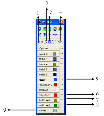
(You should be able to see the following window). Scroll down. At the bottom you should be able to see the frequently used rules. (This is for 6 metal processes. You may see a smaller list if you have selected a different foundry. No need to worry. The basic layers remain the same.)

(Click on the image to enlarge)
I will note down few of them which we will be using for this design. (Highlighted red). I suggest you to note down the same. The spacing shown is between the similar layers. The spacing between different layers may vary. But we always have DRC (Design Rule Check) to see if we are right.
Step 2:
We shall first draw p+ diffusion. We already know from the rules that it should be minimum of 4λ X 4λ. (Try drawing smaller than this and run DRC. You will become familiar with this.)
But wait, if we draw a diffusion of 4 λ by 4 λ, we won’t be able to make a proper transistor by laying polysilicon. (Minimum width of the polysilicon is 2 λ). So, we need to resize it. Click on the resize tool. (Marked with red circle). Stretch the mouse with left button clicked on the horizontal edge. (Refer to Part 1, resizing the image). Stretch it for around say 8λ and release the button. The actual minimum width required will be 12 λ (4 λ each for two contacts+ 4 λ spacing between each contacts= 8+4 = 12 λ. Note that the poly will be laid between the contact. The minimum width of poly should be 2 λ. It comfortably lies between the contacts. Illustration follows.)

(Click on the image to enlarge)

(Diffusion after stretching. Only partial diagram is shown)
Step 3:
Selecting polysilicon from the palette, draw the polysilicon layer exactly at the center of the diffusion. (Horizontal center. Poly should be vertical). Note that I have extended poly 3λ. This is to comply with the design rule. (The extra poly surrounding the diffusion should be more than 3λ).

Step 4:
Select the n-well from the palette and draw the N-well. (I love the color and pattern.) I have drawn it arbitrarily.

To make sure that we are following the design rules, click on DRC.
As you can see, the design rule says that “The extra nwell surrounding the diffp is less than 6λ.” You can directly click on the nwell and stretch it to a next level. Perform the DRC again to see if everything is fine before proceeding to the next step. One strange behavior of DRC is that, at the first click it points to the error, but even if the error is not corrected, the error message goes off. To recheck, you need to click again. One good thing about it is that, it also shows the scale. So that you can stretch or resize accordingly.
Step 5:
We are ready to draw the n diffusion now. Click on n+diffusion from the palette and draw it below p+. Keep the size same. (You can even keep it half of p+ diffusion, but since we have drawn the p+ diffusion of 4λ, we can not draw this diffusion less than that). Also maintain the distance between nwell and diffusion 6λ. Perform the DRC again. Your screen should look something similar to this:

Since in an inverter both the device gates are connected to each other, we need to extend the poly of the upper device to cover the lower device. We can also lay the poly from the palette. After this step the layout should be like:

Step 6:
Select metal layer from the palette. Join the devices (Source and Drain). Select appropriate contact from palette and click on metal-diffusion interface. Note the minimum width of the metal is maintained to 3λ. While placing the contacts, the dotted rectangle’s left edge should coincide with the left edge of the metal. Illustration:

We need to verify the contacts. Sometimes, we see the contacts, but they are not really bound. To verify, click on 2-D View. (Circled Red). Hold the left mouse button and strike diagonally over the contact. (See the dotted line on nmos). 
 

If everything goes fine, you will see the following window:

At present we are not bothered about other parameters, let us just see if there is a purple line, highlighted red. If you can see this, it means you have connected the layers successfully. If you are not able to see, then there is no need to worry. It’s not due to color blindness J close this window. Click on the connect layers button (top menu, underline yellow in last but one figure) and click on the layer you need to connect. Repeat the same for the other contact.
Step 7:
You have crossed the most rigorous part of the tutorial. If you wish to quit it now, I won’t stop. You have done 99% of it. Pat your back and let’s move ahead.
From the palette, select Vdd. Click on nwell. Again from click on vdd and then on the source of pmos. Add a contact where you have added vdd. Apply Vss to the source of the nmos in the same way. We need to apply the input to the inverter now. Select the clock from the palette and click on the poly connecting both pmos and nmos.
We should be able to see the output. For the present layout, the output will be available at the metal (joining drain and source of the devices). Click on the Visible Node (looks like an eye in the palette) and then click on the metal.
You are done now!

Step 8 (Final Step):
Click on Run Simulation button. If you have followed the tutorial properly, you will be able to see this:

You can view various simulation parameters. See the voltage vs. voltage to view the transfer characteristics.
I have uploaded the .MSK file over the following link. You can verify your design with mine and try it out.
In the next part of the tutorial, we will be learning:
  1. How to save time by using existing layout.
  2. How to Copy, paste and invert
Basically the next tutorial will be focused on design of transmission gate.

MICROWIND Tutorial Part 1 : Basic VLSI Layout Design

Hello,


In this small lab tutorial series you will be learning the use of Microwind. I appreciate yourfeedback. Feel free to express yourself.
Special thanks to my teachers and friends who helped me in learning, publishing, editing, many more tings... Thank you very much.
Grab the tool from here.
 
 
Unzip it and find the .exe file.
If you have clicked on the right icon, you should be able to see this:


(Click on the image to enlarge and see clearly)


On the right side of the window, you can see a pallet. This is your basic tool. Using palette, you can lay different layers, for example, Polysilicon, Diffusion Layer, N-Well etc.
At the top of the screen you can see various icons. Let us explore each of them one by one.
(Click on the image to enlarge and see clearly)
 
 
To make use of any of the following palette tools, click on it, and then click on the layer to which you want to apply.
 
1. Vdd Supply. This is used to supply the necessary voltage required for the layout. We usually apply this to N Well (to avoid floating) and to pMOS.
 
2 Ground. As simple as ground. It grounds the region over which it is placed.
 
3 Ads Clock to the clicked region. You can specify the period, low time, high times and many other specifications. If you are a beginner, do not change the default values. Simply click and click on the region to be applied.
Important note: Once you have applied clock to any node (point or region), the next time when you click on it to apply it to other region, it takes a period twice that of last click automatically. This happens to maintain binary counting.
 
4. Looks like an eye eh? If you want to see voltage, current or few other parameters of the node, then this is used. Usually it is used to see the output during simulation. It can also be used in debugging the layout by checking behavior of a particular node.
You can see few other buttons too. We shall come to them as and when we use them.
The next set of palette tools are to be used in a bit different way. For example, if you need a polysilicon layer, then click on Red Icon with Polysilicon written on it (They were a bit considerate to do that favor to us J ). Come to the main area (Black: Substrate) hold the left mouse button, move the mouse holdingthe left button. Ahem, much easier than MS Paint. (Try it now)
 
5. The metal 1 Layer. When you need to give metallic connection between two different parts of the layout, use this option. Please note that when you draw the metal layer over say a polysilicon, it doesn’t get connected (attached) automatically. You need to use an appropriate contact to do this. The following diagram illustrates various contacts.

(Click on the image to enlarge and see clearly)
 
6. Polysilicon. Enough kidding. Its simple.
 
7. P+ Diffusion. The substrate which we use here is P-substrate(Black Colour). We are supposed to lay it under N-well. You can draw P+ diffusion first, but make sure that you cover it with N-well. The ‘+’ sign indicates that it is doped higher than the P substrate. I recommend drawing it on the top. It won’t make any difference wherever you draw, but it increases understandability of the circuit. Follow the convention everywhere.
 
8. N+ Diffusion. I suggest drawing it in the bottom. Its same as P+. But it doesn’t need any well. You can simply place it over P-substrate (Why? :) )
 
9. The much discussed N well is ready to be drawn now! (Finally). You can lay it over P+ Diffusion. Make sure that it surrounds it completely.
 
 
You can have a look at various layers in the following figure:
 
(Click on the image to enlarge and see clearly)
 
 
It was not much difficult. In fact the whole tool is pretty simple. You have covered a major part of it. If you are a bit tired, have a cup of tea.
 
Now let us explore few tools which can enhance the layout and make it indeed a layout. I assume that by now, you have drawn at least some random blocks.
Lets have a look at the tools which are there in the top menu bar:

(Click on the image to enlarge and see clearly)


  1. Opens already existing layout. If you have saved your layout somewhere, browse to that folder and you can open it.
  2.  Save the current layout. The layouts are stored with .MSK extension. If you want to store to a specific location go to File>Save As.
  3. Its called draw box. When you click on this, then you can draw the last layer you selected from palette.
  4. Your best partner, the gun! To erase, delete or remove a particular area, click on this icon and then click on that particular layer. Tip: If you want to remove only a selected portion, first click on shoot, then hold the left mouse button and select the layer which you need to selectively remove. To completely remove more than one layer, cover them keeping the left mouse button clicked.
  5. Why to draw the same device again which you have already drawn? We have a copy tool. (Even here). Click on this, then again highlight the area by holding the left mouse key and covering that area, release the mouse button. Safely place the area where you want to. (I suggest trying this by drawing a very simple layer)
  6. Stretch (Resize)/Move tool. Yet another important tool. It is used if you want to move a certain layout from on place to another. Basically it may be contact or Vdd or Gnd etc. It can also be a layer or a complete device. If you want to move a complex layout, click on this, and again the same mouse holding trick will do it. Click once when you get satisfactory result. Resize: This is used when the design fails the design rules. You can select this and resize the layout. Click once when you get satisfactory result. Hint: If you want to resize horizontally, first click on the tool icon, go to the horizontal edge you want to resize and then draw an imaginary rectangle smaller than the edge such that it over laps the layer and substrate and resize. The same holds good for resizing vertically. (See image for illustration)
I strongly recommend you to try this by drawing a single layer. In the above figure, I am resizing the right edge of the polysilicon. You can see the rectangle in green. (gets drawn on its own when you drag the mouse by holding left key)
  1. Zoom In (Maximize) the layout. If you want to view the layout in detail, use this tool.
  2. Zoom out. I suggest using this when you are drawing a large layout. Zoom out to connect the devices in proper alignment.
  3. See All. As it says, it fits your layout to the screen.
  4. It shows the electrical properties. (You will not be using it initially, so don’t worry)
  5. Run Simulation: Click this when you are done. It shows the various input and output waveform. (We will come to this in the next part)
  6. Measures the distance of various layers, devices. If you know the design rule, use it repeatedly to verify you adhere to them
  7. 2-D cross section. As the name indicates, it shows the 2-Dimensionla view of the selected area. Hint: After connecting two layer, say polysilicon and metal, with a contact, you need to make sure that both the layers are connected. You will get erroneous results if they fail to connect properly. In such a case, click on this tool and then hold the right mouse button and drag it till you cover the contact. It clearly indicates if the layers are connected. Diagram illustrates the same.   
  8. This gives 3-D view of the layout. Try this out, looks good! J
  9. DRC: Design Rule Check. It check various design rules and suggest corrections if the rules are violated. Hint: It is recommended to perform the DRC after laying each and every layer. This helps you to debug the circuit easily. Also try to use as less amount of diffusions or silicon as possible. Remember: In silicon real estate, every nano meter is precious. Not only that, it prevents unwanted capacitance and resistance
  10. Add text. This is like commenting code in programming language. It helps to make your layout readable. Click on this tool and click where you want to add the text.
  11. Connect Layers: Suppose you have drawn two layers, and want to interconnect (they are not connected by default) click on this and then on the layers.
  12. This simulates MOS characteristics.
  13. Show Palette. It happens. Sometimes, the palette disappears. (I don’t know why). To get it back, click on this.
  14. To scroll around the layout, to see various areas, use these arrows.
Tip: Use Ctrl+U to undo.
Congratulations!
You have successfully completed the first part of the tutorial.