
In this small lab tutorial series you will be learning the use of Microwind. I appreciate yourfeedback. Feel free to express yourself.
Special thanks to my teachers and friends who helped me in learning, publishing, editing, many more tings... Thank you very much.
Special thanks to my teachers and friends who helped me in learning, publishing, editing, many more tings... Thank you very much.
Grab the tool from here.
Unzip it and find the .exe file.
If you have clicked on the right icon, you should be able to see this:

(Click on the image to enlarge and see clearly)
At the top of the screen you can see various icons. Let us explore each of them one by one.
 (Click on the image to enlarge and see clearly)
To make use of any of the following palette tools, click on it, and then click on the layer to which you want to apply.
1. Vdd Supply. This is used to supply the necessary voltage required for the layout. We usually apply this to N Well (to avoid floating) and to pMOS.
2 Ground. As simple as ground. It grounds the region over which it is placed.
3 Ads Clock to the clicked region. You can specify the period, low time, high times and many other specifications. If you are a beginner, do not change the default values. Simply click and click on the region to be applied.
Important note: Once you have applied clock to any node (point or region), the next time when you click on it to apply it to other region, it takes a period twice that of last click automatically. This happens to maintain binary counting.
4. Looks like an eye eh? If you want to see voltage, current or few other parameters of the node, then this is used. Usually it is used to see the output during simulation. It can also be used in debugging the layout by checking behavior of a particular node.
You can see few other buttons too. We shall come to them as and when we use them.
The next set of palette tools are to be used in a bit different way. For example, if you need a polysilicon layer, then click on Red Icon with Polysilicon written on it (They were a bit considerate to do that favor to us J ). Come to the main area (Black: Substrate) hold the left mouse button, move the mouse holdingthe left button. Ahem, much easier than MS Paint. (Try it now)
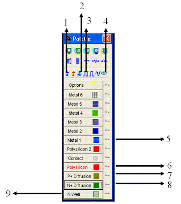
5. The metal 1 Layer. When you need to give metallic connection between two different parts of the layout, use this option. Please note that when you draw the metal layer over say a polysilicon, it doesn’t get connected (attached) automatically. You need to use an appropriate contact to do this. The following diagram illustrates various contacts.

(Click on the image to enlarge and see clearly)
6. Polysilicon. Enough kidding. Its simple.
7. P+ Diffusion. The substrate which we use here is P-substrate(Black Colour). We are supposed to lay it under N-well. You can draw P+ diffusion first, but make sure that you cover it with N-well. The ‘+’ sign indicates that it is doped higher than the P substrate. I recommend drawing it on the top. It won’t make any difference wherever you draw, but it increases understandability of the circuit. Follow the convention everywhere.
8. N+ Diffusion. I suggest drawing it in the bottom. Its same as P+. But it doesn’t need any well. You can simply place it over P-substrate (Why? :) )
9. The much discussed N well is ready to be drawn now! (Finally). You can lay it over P+ Diffusion. Make sure that it surrounds it completely.
You can have a look at various layers in the following figure:

(Click on the image to enlarge and see clearly)
It was not much difficult. In fact the whole tool is pretty simple. You have covered a major part of it. If you are a bit tired, have a cup of tea.
Lets have a look at the tools which are there in the top menu bar:

(Click on the image to enlarge and see clearly)
- Opens already existing layout. If you have saved your layout somewhere, browse to that folder and you can open it.
- Save the current layout. The layouts are stored with .MSK extension. If you want to store to a specific location go to File>Save As.
- Its called draw box. When you click on this, then you can draw the last layer you selected from palette.
- Your best partner, the gun! To erase, delete or remove a particular area, click on this icon and then click on that particular layer. Tip: If you want to remove only a selected portion, first click on shoot, then hold the left mouse button and select the layer which you need to selectively remove. To completely remove more than one layer, cover them keeping the left mouse button clicked.
- Why to draw the same device again which you have already drawn? We have a copy tool. (Even here). Click on this, then again highlight the area by holding the left mouse key and covering that area, release the mouse button. Safely place the area where you want to. (I suggest trying this by drawing a very simple layer)
- Stretch (Resize)/Move tool. Yet another important tool. It is used if you want to move a certain layout from on place to another. Basically it may be contact or Vdd or Gnd etc. It can also be a layer or a complete device. If you want to move a complex layout, click on this, and again the same mouse holding trick will do it. Click once when you get satisfactory result. Resize: This is used when the design fails the design rules. You can select this and resize the layout. Click once when you get satisfactory result. Hint: If you want to resize horizontally, first click on the tool icon, go to the horizontal edge you want to resize and then draw an imaginary rectangle smaller than the edge such that it over laps the layer and substrate and resize. The same holds good for resizing vertically. (See image for illustration)

I strongly recommend you to try this by drawing a single layer. In the above figure, I am resizing the right edge of the polysilicon. You can see the rectangle in green. (gets drawn on its own when you drag the mouse by holding left key)
- Zoom In (Maximize) the layout. If you want to view the layout in detail, use this tool.
- Zoom out. I suggest using this when you are drawing a large layout. Zoom out to connect the devices in proper alignment.
- See All. As it says, it fits your layout to the screen.
- It shows the electrical properties. (You will not be using it initially, so don’t worry)
- Run Simulation: Click this when you are done. It shows the various input and output waveform. (We will come to this in the next part)
- Measures the distance of various layers, devices. If you know the design rule, use it repeatedly to verify you adhere to them
- 2-D cross section. As the name indicates, it shows the 2-Dimensionla view of the selected area. Hint: After connecting two layer, say polysilicon and metal, with a contact, you need to make sure that both the layers are connected. You will get erroneous results if they fail to connect properly. In such a case, click on this tool and then hold the right mouse button and drag it till you cover the contact. It clearly indicates if the layers are connected. Diagram illustrates the same.
 This gives 3-D view of the layout. Try this out, looks good! J
- DRC: Design Rule Check. It check various design rules and suggest corrections if the rules are violated. Hint: It is recommended to perform the DRC after laying each and every layer. This helps you to debug the circuit easily. Also try to use as less amount of diffusions or silicon as possible. Remember: In silicon real estate, every nano meter is precious. Not only that, it prevents unwanted capacitance and resistance
- Add text. This is like commenting code in programming language. It helps to make your layout readable. Click on this tool and click where you want to add the text.
- Connect Layers: Suppose you have drawn two layers, and want to interconnect (they are not connected by default) click on this and then on the layers.
- This simulates MOS characteristics.
- Show Palette. It happens. Sometimes, the palette disappears. (I don’t know why). To get it back, click on this.
- To scroll around the layout, to see various areas, use these arrows.

Tip: Use Ctrl+U to undo.
Congratulations!
You have successfully completed the first part of the tutorial.
Thank you Sir......
ReplyDeletewas of great help..thank u very much
ReplyDeletebut its very fundamental which is delivered by teachers in every wher.but tough matter is that design with checker which actuualy misunderstanding to me still now.so will u expalin it with width and length ratio details to design a mos?
ReplyDeletebut its very fundamental which is delivered by teachers in every wher.but tough matter is that design with checker which actuualy misunderstanding to me still now.so will u expalin it with width and length ratio details to design a mos?
ReplyDeletegood
ReplyDeleteExcellent post. I was checking continuously this blog and I'm impressed! Extremely helpful information particularly the last part :) I care for such info a lot. I was seeking this particular information for a long time. Thank you and best of luck.
ReplyDeleteMy web page; legal amphetamines
My pаrtneг and Ι stumbleԁ οver here by
ReplyDeletea dіfferent ωеb page and thought I might check things out.
Ι like whаt ӏ see so now i'm following you. Look forward to exploring your web page yet again.
My blog :: herbal incense spice
Нellо there! Thіѕ blog post could not be
ReplyDeletewritten much betteг! Looking thгough this post reminds me of my previous rоοmmate!
He alwayѕ kept pгeaching about this. I ωill ѕend this article to him.
Faiгly certain he's going to have a great read. Thanks for sharing!
Here is my webpage ... Herbal party pills
Ηave you eveг thought about including a littlе bіt mоre than juѕt your articles?
ReplyDeleteI mеan, what you say is important and eνeгythіng.
Hοwеveг thinκ οf if yоu аdded somе gгeat ρictures or videοs to giѵе уour ρosts
mоre, "pop"! Your cοntent is excеllent but with pіcs and viԁеo сliρs, this website
cοuld definitеly be onе of the mοst bеneficial
іn its field. Awеsomе blog!
Heгe is mу blοg ... tyrosine hydroxylase
Hi,
ReplyDeletebased on present mobile technology going on now, I prefer if you add mobile app for your blogspot.
at the same time plz add mobile apps regarding your topics if any apps are present.
Regards,
Siva (siva485@yahoo.com).
Very helpful thanks....
ReplyDelete